


Gold Finger Pcb
SPCB002
Gold finger pcb.The gold finger is composed of a plurality of golden conductive contacts. Because the surface is gold-plated and the conductive contacts are arranged like a finger, it is called a "golden finger". The gold finger is actually coated with a layer of gold on a copper clad plate by a special process because gold is highly resistant to oxidation and has high conductivity. Since the 1990s, Tin materials have become popular. At present, the "golden fingers" of motherboards, memory and graphics cards are almost always used Tin material.
Quantity:
0.00
Unable to ship to shipping address, please feedback to us
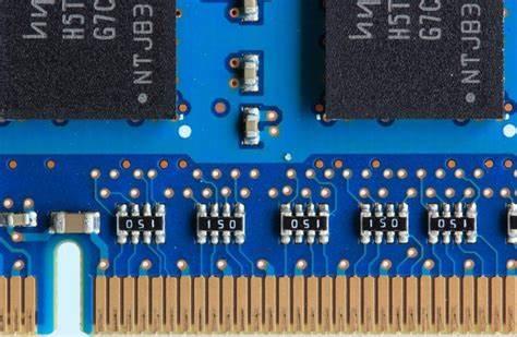
In today’s computerized and mobile-activated world, signals are sent between numerous devices. For each command to be enacted, communication must be made between two or more circuit boards. None of this would be possible without gold fingers, which serve as the connecting contacts between motherboards and components like graphics or sound cards.
Gold fingers are the gold-plated columns that you see along the connecting edges of printed circuit boards (PCBs). The purpose of gold fingers is to connect a secondary PCB to the motherboard of a computer. PCB gold fingers are also used in various other devices that communicate via digital signals, such as smartphones and smartwatches. Gold is used for the connecting points along a PCB because of the alloy’s superior conductivity.
There are two types of gold applicable to the PCB gold finger plating process:
- Electroless Nickel Immersion Gold (ENIG): This gold is more cost-effective and easier to solder than electroplated gold, but its soft, thin (typically 2-5u” composition renders ENIG unsuitable for the abrasive effects of circuit board insertion and removal.
- Electroplated Hard gold: This gold is solid (hard) and thick (typically 30u”), thus more ideal for the abrasive effects of constant PCB usage.
Gold fingers are used as connecting contacts between two adjoining PCBs. Aside from its conductivity, the purpose of the gold is to protect the connecting edges from wear over many uses. Due to the strength of hard gold at its specified thickness, gold fingers make it possible for a PCB to be connected, disconnected and reconnected up to 1,000 different times in a corresponding slot.
The functions of gold fingers are multi-purpose. With any given computer setup, you will see a number of peripherals that connect with the computer itself thanks to PCB gold fingers. Some of the most widespread uses of gold fingers include the following:
- Interconnection points: When a secondary PCB connects to the main motherboard, it is done through one of several female slots, such as a PCI, ISA or AGP slot. Through these slots, the gold fingers conduct signals between a peripheral device or an internal card and the computer itself.
- Special adapters: Gold fingers make it possible to add numerous performance enhancements to a personal computer. Through secondary PCBs that slot perpendicular into the motherboard, a computer can deliver enhanced graphics and hi-fidelity sound. Since these cards are seldom unattached and reattached, the gold fingers generally outlast the card itself.
- External connections: The outer peripherals that have been added to a computer station are connected to the motherboard with PCB gold fingers. Devices such as speakers, subwoofers, scanners, printers and monitors are all plugged into specific slots behind the computer tower. These slots, in turn, attach to PCBs that connect to the motherboard.
Gold finger pcb producing capability
| Item | Specification |
| Numbr of Layer | 1-28 Layers |
| Material | FR4,CEM-1/CEM-3,ROGERS and so on |
| Surface Finish | HASL, Gold plating, Enig,Immersion gold, Immersion Tin, OSP |
| Finish Board Thickness | 0.2mm-6.00 mm(8mil-126mil) |
| Copper Thickness | 0.5 oz ~12 oz max |
| Solder Mask | Green/Black/White/Red/Blue |
| Min.Trace Width & Line Spacing | 0.075mm/0.1mm(3mil/4mil) |
| Min.Hole Diameter for CNC Driling | 0.1mm(4mil) |
| Min.Hole Diameter for punching | 0.9mm(35mil) |
| Biggest panel size | 610mm*508mm |
| Hole Positon | +/-0.075mm(3mil) CNC Driling |
| Conductor Width(W) | 0.05mm(2mil)or;+/-20% of original artwork |
| Hole Diameter(H) | PTH L:+/-0.075mm(3mil);Non-PTH L:+/-0.05mm(2mil) |
| Outline Tolerance | 0.125mm(5mil) CNC Routing;+/-0.15mm(6mil) by Punching |
| Warp & Twist | 0.70% |
| Insulation Resistance | 10Kohm-20Mohm |
| Conductivity | <50ohm |
| Test Voltage | 10-300V |
| Panel Size | 110×100mm(min);660×600mm(max) |
| Layer-layer misregistration | 4 layers:0.15mm(6mil)max;6 layers:0.25mm(10mil)max |
| Min.spacing between hole edge to circuity pattern of an inner layer | 0.25mm(10mil) |
| Min.spacing between board ouline to circuitry pattern of an inner layer | 0.25mm(10mil) |
| Board thickness tolerance | 4 layers:+/-0.13mm(5mil);6 layers:+/-0.15mm(6mil) |
| Impedance Control | +/-10% |
| Different Impendance | +-/10% |
Quote requirement:
1,Design files (Gerber files, drill and readme file in a zip or rar packaged; or BOM list)
2.Clear quantity of pcb sample for us
3,Test method for PCBA
Workshop:

FAQ:
1. Can you keep my design file secure ?
Your files are held in complete safety and security.Your files are never shared nor will any third parties have access to your design files.We can sign an NDA(Non-disclosure agreement) before sending files.
2. For small quantity orders, can you produce prototype PCBs?
Yes. we can produce prototypes. and the more quantity, the more cost savings.
3. What file formats do you accept for PCB and assembly?
Gerber ,CAM Auto CAD DXF, DWG formats.
4. Do you have after-sales product servicing available for your customers?
Yes, for any quality problems, we will take our responsibility to solve it for you any time.
Recommend Products


