


Routing Peelable ceramic substrate printed board pcb
- Model Number:Ceramic PCB
- Place of Origin:Guangdong, China
- Brand Name:XingDa
- Base Material:Ceramic/Alumina 99.5%/Alumina 99%
- Copper Thickness:3 OZ
- Board Thickness:0.2mm-6.00 mm(8mil-126mil)
- Min. Hole Size:0.1mm(4mil)
- Min. Line Width:0.075mm(3mil)
- Min. Line Spacing:0.1mm(4mil)
- Surface Finishing:Gold, silver
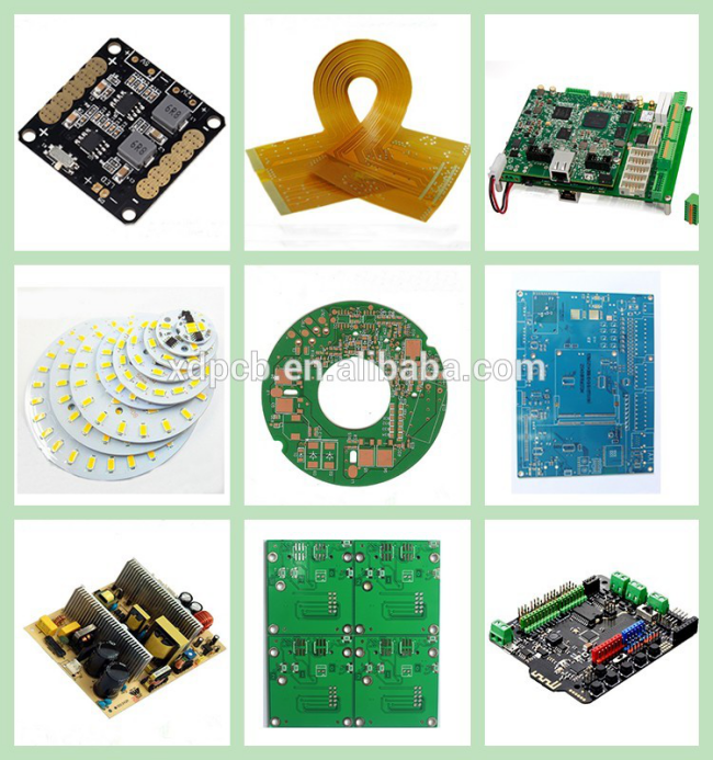
- gold-plated pcb ::half-hole pcb
- HDI pcb::via-in-pad pcb
- impedance control pcb::pcb smt assembly
- Item:Ceramic pcb
Routing Peelable ceramic substrate printed board pcb
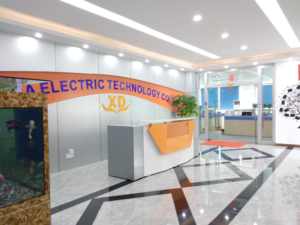
Welcome to XingDa Electric Technology Co.,Ltd
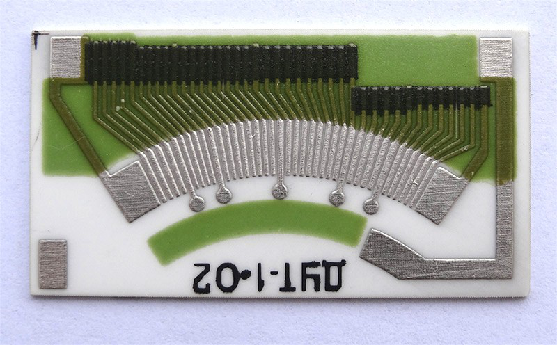
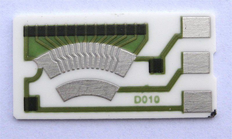
Item | Test Condition | unite | senior |
material | Ceramic/Aluminium nitride Ceramic /Alumina 99.5%/Alumina 99% | ||
Color status |
|
|
|
average crystal size |
| μm | 3-5 |
volume density |
| g/cm2 | >3.74 |
water absorption |
| % | 0 |
Vickers hardness | Load 4.9 | Gpa | >15 |
flexural Strength | Bending moment 80mm | Mpa | >324 |
Linear Coefficient of Thermal Expansion | 20-500℃ 20-800℃ | 1×10- mm/℃ | 605-7.5 6.5-8.0 |
thermal conductivity | 20℃ | W(m-k) | >170 |
Dielectric intensity |
| Kv/mm | >12 |
Volume Resistance | 20℃ 300℃ 500℃ | -cm
| >1014 >1011 >109 |
Dielectric Constant | 1MHz |
| 9.3-10.6 |
dielectric loss | 1MHz |
| 3×10⁻⁴ |
Thermal - shock | 850℃ | times | >7 |
roughness of the surface | Ra(λ2) | μm | 0.20-0.75 |
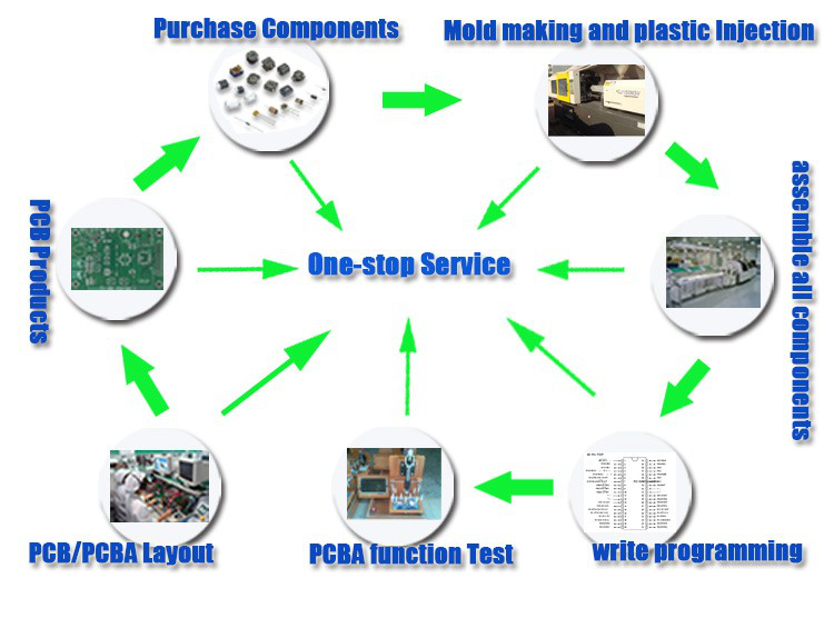
One-stop OEM ODM PCBA manufacturer
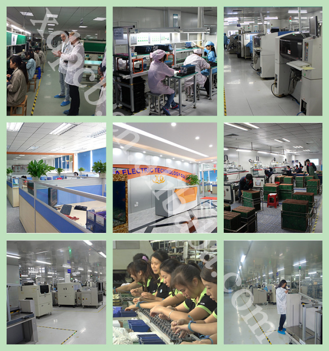
We are professional manufacturer in various PCB and PCBA with 9 years experience, we can provide a reasonable price with high quality products.
SMT Capacity | |
SMT Item | Capacity |
PCB Max. size | 510mm*460mm(SMT) |
Chip component | 0805 0603 0402 0201 package |
Min.pin space of IC | 0.1mm |
Min. space of BGA | 0.1mm |
Max.precision of IC assembly | ±0.03mm |
Assembly capacity | ≥8 million piots/day |
DIP capacity | 6 DIP production lines |
Assembly testing | Bridge test,AOI test, X-Ray test, ICT(In Circuit Test),FCT (Functional Circuit Test) |
| Current test, voltage test, high temperature and low temperature test, Drop Impact Test,aging test, water proof test,leakage-proof test and etc. Different test can be done according to your requirement. |
Details for Ceramic PCB:
Technical
1). Professional surface mounting and through hole soldering technology;
2). Various sizes, like 1206, 0805, 0603, 0402, 0102 components SMT technology;
3). X-Ray, ICT(In Circuit Test), FCT(Functional Circuit Test) technology;
4). Nitrogen gas reflow soldering technology for SMT;
5). High standard SMT&Solder Assembly line;
6). High density interconnected board placement technology capacity.
9 years focus on high quality Ceramic PCB, FPC and PCBA!
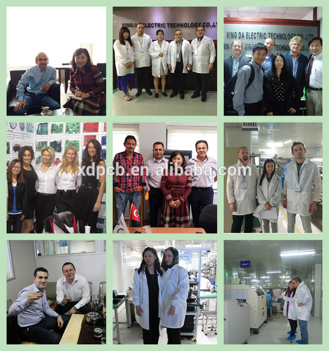
Customer visiting
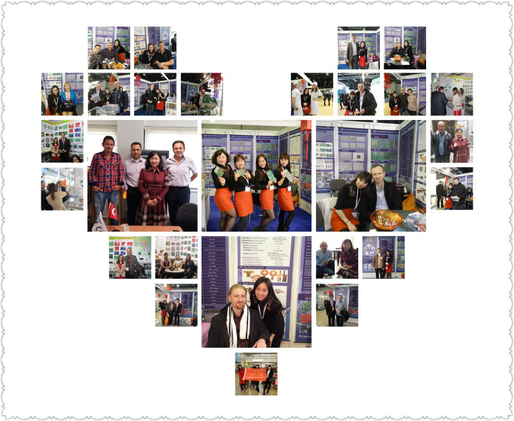
Exhibition Show:
Q1: Are you a factory or trade company?
A: XingDa is a PCB/FPC/PCBA manufacturer/factory. We pecialize in PCB/PCBs Board for 9 years.
Q2: Is my PCB file safe if I send it to you for manufacturing?
A: We respect customer's design authority and will never manufacture PCB for someone else without your permission. NDA is acceptable.
Q3: What payment do you accept ?
A: TT/ Western Union/ Paypal/ Unistream.
Q4: What's your shipping way ?
A: 1. We have our own forwarder to ship goods by DHL, UPS, FEDEX, TNT,EMS.
2. If you have your own forwarder, we can cooperate with them.
Q5: How about the MOQ?
A: For PCB: 1 pcs
For PCBA: 1000pcs
Q6: What's your main market?
A: Europe, USA, Brazil, Russia, Turkey, Austrialia, Singapore...

 Single-sided quartz glass substrate Alumina Ceramic PCBs Biomedical testing 3D printer insulation bed, ceramic substrate luminous keyboard motherboard, alumina pcb grating gear
 High frequency and high speed circuit substrate ceramic pcb Characteristic impedance 50Ω ceramic printed circuit board differential impedance 100Ω ceramic substrate pcb circuit board
 1.0mm Ceramic Circuit Board ENIG alumina circuit board High frequency and high speed printed circuit board ceramic pcb board
 2 layers al203 ceramic pcb printed circuit boards