


Custom pcb for high power amplifier circuit board
PCB-11
Most high-power RF applications have thermal management issues, and good thermal management needs to consider some basic relationships. For example, the relationship with loss, when the input signal power in the circuit, the higher the loss of the circuit will generate higher heat; the other is related to the frequency, the higher the frequency will generate more heat. In addition, the increase of heat in any dielectric material will cause a change in the Dk (dielectric constant) of the dielectric material, that is, the temperature coefficient of dielectric constant (TCDk). As the loss changes lead to changes in circuit temperature, changes in temperature lead to changes in Dk. This Dk change caused by TCDk will affect the performance of the RF circuit and may affect system applications.
Quantity:
0.00
Unable to ship to shipping address, please feedback to us
Custom pcb for high power amplifier circuit board
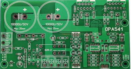
The signal is first amplified and then processed by the microcontroller to produce an output.
It is used to convert analog signals to square waves with high input saturation. The waveform shaping phenomenon takes advantage of harmonic saturation. It helps to convert the signal into a square wave.
The amplifier PCB is also essential in increasing the signal amplitude. In this exercise, it further helps to maintain other aspects, such as frequency.
They have high voltage gain and almost high output resistance. This feature allows them to provide enough output to drive speakers.
There is almost no gain due to their low input resistance. In this regard, it acts as a buffer between the circuit and the receiver. It helps prevent unwanted signals.
High-frequency amplifier PCBs help detect metal fatigue. They also facilitate ultrasonic cleaning, ultrasonic scanning and remote control of sensors.
Amplifier PCBs with constant gain between DC and AC are used in oscilloscopes. It is due to the level of accuracy required to measure the signal over the entire frequency range.
The buffer type is used between two circuits to prevent interference operation of one to the other. They also help with impedance matching. This is because they have high input impedance and low output impedance.
Product Description
Amplifier PCBs
Amplifier PCBs can be used in a variety of applications. This is because, in most cases, they constitute the central operating point for converting the original analog signal into a digital signal.The signal is first amplified and then processed by the microcontroller to produce an output.
It is used to convert analog signals to square waves with high input saturation. The waveform shaping phenomenon takes advantage of harmonic saturation. It helps to convert the signal into a square wave.
The amplifier PCB is also essential in increasing the signal amplitude. In this exercise, it further helps to maintain other aspects, such as frequency.
They have high voltage gain and almost high output resistance. This feature allows them to provide enough output to drive speakers.
There is almost no gain due to their low input resistance. In this regard, it acts as a buffer between the circuit and the receiver. It helps prevent unwanted signals.
High-frequency amplifier PCBs help detect metal fatigue. They also facilitate ultrasonic cleaning, ultrasonic scanning and remote control of sensors.
Amplifier PCBs with constant gain between DC and AC are used in oscilloscopes. It is due to the level of accuracy required to measure the signal over the entire frequency range.
The buffer type is used between two circuits to prevent interference operation of one to the other. They also help with impedance matching. This is because they have high input impedance and low output impedance.
Product Description
| Item | Technical Parameters | Specification |
| Layers | 1-22 layers | _ |
| Min. line width | 2/2mil | Partial 2mil lines is allowed |
| Min. line space | 2/2mil | Partial 2mil lines is allowed |
| Min.annular ring width: vias | 3mil | _ |
| Min.annular ring width: component holes | 7mil | _ |
| Min.hole size(board thickness <2mm) | 4mil | _ |
| Min.hole size(board thickness ≥2mm) | Aspect ratio≤16 | _ |
| Max.board thickness(single&doule sided) | 6mm | _ |
| Max.board thickness(multilayer) | 8mm | _ |
| Min.board thickness(single&doule sided) | 0.2mm | _ |
| Min.board thickness(multilayer) | 4layers:0.4mm;6layers:0.6mm;8layers:1mm; 10layers:1.2mm | _ |
| Max.board size (single&doule sided) | 700*1200mm | _ |
| Max.board size (multilayer) | 700*1200mm | _ |
| Distance between line to board edge | Outline: 0.2mm V-CUT: 0.4mm | _ |
| Solder mask bridge | 4mil | Between IC pins |
| Solder mask color | White,black,blue,green,yellow,red,ect | _ |
| Legend color | White,black,yellow,ect | _ |
| Surface finish | HAL(with Pb free),plated Ni/Au,Immersion silver,Imm Ni/Au,Imm Sn, hard gold,OSP,ect | _ |
| Plating thickness(Technique: hard gold) | Plating type: Ni, Min./Max thickness:100/150U'' Plating type: Au, Min./Max thickness:5/120U'' | _ |
| Plating thickness (Technique:Immersion Ni/Au) | Plating type: Imm Ni, Min./Max thickness:100/150U'' Plating type: Imm Au, Min./Max thickness:2/4U'' | _ |
| Plating thickness (Technique: gold finger) | Plating type: Ni, Min./Max thickness:120/150U'' Plating type: Au, Min./Max thickness:5/120U'' | _ |
| Copper plating hole | Copper thickness: Min.20um/Max.25um | _ |
| Base copper thickness(Inner and outer layer) | Min. thickness:1/3 OZ Max.thickness:6OZ | _ |
| Finished copper thickness | Outer layers: Min.thickness 1 OZ,Max.thickness 10 OZ Inner layers: Min.thickness 0.5 OZ,Max.thickness 6 OZ | _ |
Recommend Products
 Angle position sensor carbon printing pcb carbon circuit board batch PCB printed circuit board
 Single-sided quartz glass substrate Alumina Ceramic PCBs Biomedical testing 3D printer insulation bed, ceramic substrate luminous keyboard motherboard, alumina pcb grating gear
 High frequency and high speed circuit substrate ceramic pcb Characteristic impedance 50Ω ceramic printed circuit board differential impedance 100Ω ceramic substrate pcb circuit board
 1.0mm Ceramic Circuit Board ENIG alumina circuit board High frequency and high speed printed circuit board ceramic pcb board