


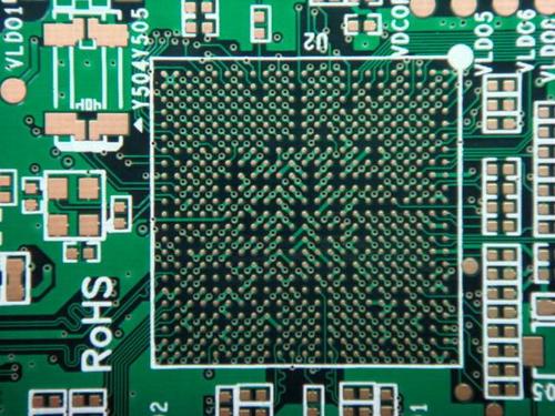
BGA pads pcb for pcb prototype and mass production
PCB-7
PADS is a PCB design package developed by Mentor Graphics. It comes in three trim levels (Standard, Standard Plus, and Professional) and is considered a high-end commercial-grade package. It has many high-end features, including signal integrity analysis capabilities, advanced autorouter, thermal design consideration analysis, and support for various project management functions.
Quantity:
US $0.00
Unable to ship to shipping address, please feedback to us
BGA pads pcb for pcb prototype and mass production
Welcome to XingDa Electric Technology Co.,Ltd
Best BGA PCB Prototype Circuit Board manufacture services
A PCB Prototype is an early sample, model, or release of a product built to test a concept or process or to act as a thing to be replicated or learned from. A PCB Prototype is generally used to evaluate a new design to enhance precision by system analysts and users. Prototyping serves to provide specifications for a real, working system rather than a theoretical one. In some design workflow models, creating a prototype (a process sometimes called materialization) is the step between the formalization and the evaluation of an idea .
The BGA is descended from the pin grid array (PGA), which is a package with one face covered (or partly covered) with pins in a grid pattern which, in operation, conduct electrical signals between the integrated circuit and the Printed Circuit Board ( BGA PCB Prototype) on which it is placed. In a BGA the pins are replaced by pads on the bottom of the package, each initially with a tiny solder ball stuck to it. These solder spheres can be placed manually or by automated equipment, and are held in place with a tacky flux. The device is placed on a PCB with copper pads in a pattern that matches the solder balls. The assembly is then heated, either in a reflow oven or by an infrared heater, melting the balls. Surface tension causes the molten solder to hold the package in alignment with the circuit board, at the correct separation distance, while the solder cools and solidifies, forming soldered connections between the device and the PCB.
In more advanced technologies, solder balls may be used on both the PCB and the package. Also, in stacked multi-chip modules, solder balls are used to connect two packages.
We can provide one-stop service:
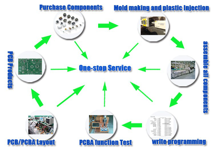
1. PCB circuit boards.
2. E-test.
3.Electronic components purchasing.
4. PCB assembly: available on SMT, BGA, DIP.
5. PCBA function test.
6. Enclosure assembly.
PCB product Capacity
FAQ
Q1:Are you a factory or trade company?
A: XingDa is a PCB/FPC/PCBA manufacturer/factory. We specialize in PCB/PCBs Board 10years.
Q2:Is my PCB file safe if I send it to you for manufacturing?
A: We respect customer's design authority and will never manufacture PCB for someone else without your permission. NDA is acceptable.
Q3:What payment do you accept ?
A: TT/ Western Union/ Paypal/ L/C.
Q4: What's your shipping way ?
A: 1. We have our own forwarder to ship goods by DHL, UPS, FEDEX, TNT,EMS.
2. If you have your own forwarder, we can cooperate with them.
Q5: How about the MOQ?
A: For PCB: 1 pcs
For PCBA: 1pcs
Welcome to XingDa Electric Technology Co.,Ltd
Best BGA PCB Prototype Circuit Board manufacture services
A PCB Prototype is an early sample, model, or release of a product built to test a concept or process or to act as a thing to be replicated or learned from. A PCB Prototype is generally used to evaluate a new design to enhance precision by system analysts and users. Prototyping serves to provide specifications for a real, working system rather than a theoretical one. In some design workflow models, creating a prototype (a process sometimes called materialization) is the step between the formalization and the evaluation of an idea .
The BGA is descended from the pin grid array (PGA), which is a package with one face covered (or partly covered) with pins in a grid pattern which, in operation, conduct electrical signals between the integrated circuit and the Printed Circuit Board ( BGA PCB Prototype) on which it is placed. In a BGA the pins are replaced by pads on the bottom of the package, each initially with a tiny solder ball stuck to it. These solder spheres can be placed manually or by automated equipment, and are held in place with a tacky flux. The device is placed on a PCB with copper pads in a pattern that matches the solder balls. The assembly is then heated, either in a reflow oven or by an infrared heater, melting the balls. Surface tension causes the molten solder to hold the package in alignment with the circuit board, at the correct separation distance, while the solder cools and solidifies, forming soldered connections between the device and the PCB.
In more advanced technologies, solder balls may be used on both the PCB and the package. Also, in stacked multi-chip modules, solder balls are used to connect two packages.
We can provide one-stop service:
1. PCB circuit boards.
2. E-test.
3.Electronic components purchasing.
4. PCB assembly: available on SMT, BGA, DIP.
5. PCBA function test.
6. Enclosure assembly.
PCB product Capacity
| PCB Manufacture Capacity | |
| Item | Specification |
| Material | FR-4, FR1,FR2; CEM-1, CEM-3,Rogers, Teflon,Arlon,Aluminum Base, Copper Base,Ceramic, Crockery, etc. |
| Remarks | High Tg CCL is Available(Tg>=170℃) |
| Finish Board Thickness | 0.2 mm-6.00mm(8mil-126mil) |
| Surface Finish | Gold finger(>=0.13um), Immersion Gold(0.025-0075um), Plating Gold(0.025-3.0um), HASL(5-20um), OSP(0.2-0.5um) |
| Shape | Routing,Punch,V-cut,Chamfer |
| Surface Treatment | Solder Mask(black, green, white, red, blue, thickness>=12um, Block, BGA) |
| Silkscreen(black, yellow, white) | |
| Peel able-mask(red, blue, thickness>=300um) | |
| Minimum Core | 0.075mm(3mil) |
| Copper Thickness | 1/2 oz min; 12oz max |
| Min Trace Width & Line Spacing | 0.075mm/0.075mm(3mil/3mil) |
| Min Hole Diameter for CNC Drilling | 0.1mm(4mil) |
| Min Hole Diameter for Punching | 0.6mm(35mil) |
| Biggest panel size | 610mm * 508mm |
| Hole Position | +/-0.075mm(3mil) CNC Drilling |
| Conductor Width(W) | +/-0.05mm(2mil) or +/-20% of original |
| Hole Diameter(H) | PTHL:+/-0.075mm(3mil) |
| Non PTHL:+/-0.05mm(2mil) | |
| Outline Tolerance | +/-0.1mm(4mil) CNC Routing |
| Warp & Twist | 0.70% |
| Insulation Resistance | 10Kohm-20Mohm |
| Conductivity | <50ohm |
| Test Voltage | 10-300V |
| Panel Size | 110 x 100mm(min) |
| 660 x 600mm(max) | |
| Layer-layer misregistration | 4 layers:0.15mm(6mil)max |
| 6 layers:0.25mm(10mil)max | |
| Min spacing between hole edge to circuitry pattern of an inner layer | 0.25mm(10mil) |
| Min spacing between board outline to circuitry pattern of an inner layer | 0.25mm(10mil) |
| Board thickness tolerance | 4 layers:+/-0.13mm(5mil) |
FAQ
Q1:Are you a factory or trade company?
A: XingDa is a PCB/FPC/PCBA manufacturer/factory. We specialize in PCB/PCBs Board 10years.
Q2:Is my PCB file safe if I send it to you for manufacturing?
A: We respect customer's design authority and will never manufacture PCB for someone else without your permission. NDA is acceptable.
Q3:What payment do you accept ?
A: TT/ Western Union/ Paypal/ L/C.
Q4: What's your shipping way ?
A: 1. We have our own forwarder to ship goods by DHL, UPS, FEDEX, TNT,EMS.
2. If you have your own forwarder, we can cooperate with them.
Q5: How about the MOQ?
A: For PCB: 1 pcs
For PCBA: 1pcs
Recommend Products
 Angle position sensor carbon printing pcb carbon circuit board batch PCB printed circuit board
 Single-sided quartz glass substrate Alumina Ceramic PCBs Biomedical testing 3D printer insulation bed, ceramic substrate luminous keyboard motherboard, alumina pcb grating gear
 High frequency and high speed circuit substrate ceramic pcb Characteristic impedance 50Ω ceramic printed circuit board differential impedance 100Ω ceramic substrate pcb circuit board
 1.0mm Ceramic Circuit Board ENIG alumina circuit board High frequency and high speed printed circuit board ceramic pcb board