


6 layers pcb motherboard pcb board manufacturer
PCB-1
Proper stacking of 6-layer PCB manufacturers can help you achieve better performance as it will help suppress EMI, use various types of RF equipment and include several fine pitch components
As 6-layer PCB manufacturing technology matures, customers are increasingly concerned about the cost of large-scale 6-layer PCB manufacturing. The XDX circuit is a 6 layer PCB
manufacturer. XDX Circuits has a highly automated multi-layer PCB manufacturing facility that meets the delivery and quality requirements of 6-layer boards produced by customers and further
Reduce manufacturing costs for 6-layer PCB prototypes.
Quantity:
0.00
Unable to ship to shipping address, please feedback to us
6 layers pcb motherboard pcb board manufacturer
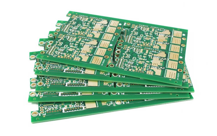
The benefits of using a 6-layer PCB
1. Small footprint: Due to their multi-layer design, these printed circuit boards are smaller than others. This is especially beneficial for tiny devices.
2. Quality-Oriented Design: 6-layer PCB stack-up design requires a lot of planning. This helps reduce errors in detail, ensuring a high-quality build. Additionally, all major PCB manufacturers today employ various testing and inspection techniques to ensure the suitability of these boards.
3. Lightweight construction: Compact PCBs are being achieved by using lightweight components, which help to reduce the overall weight of the PCB. Unlike single-layer or double-layer PCBs, 6-layer boards do not require multiple connectors to interconnect components.
4. Increased Durability: These PCBs use multiple insulating layers between circuits that are bonded using protective materials and different prepreg adhesives. This helps improve the durability of these PCBs.
5. Excellent electrical properties: These printed circuit boards have excellent electrical properties to ensure high speed and high capacity in a compact design.


Packing
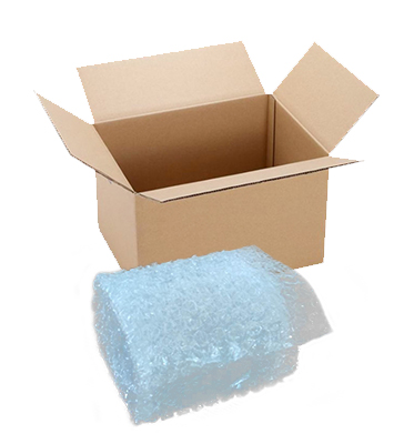
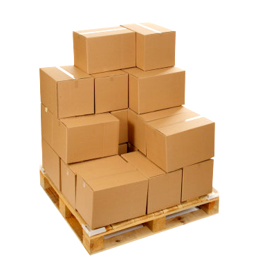
The benefits of using a 6-layer PCB
1. Small footprint: Due to their multi-layer design, these printed circuit boards are smaller than others. This is especially beneficial for tiny devices.
2. Quality-Oriented Design: 6-layer PCB stack-up design requires a lot of planning. This helps reduce errors in detail, ensuring a high-quality build. Additionally, all major PCB manufacturers today employ various testing and inspection techniques to ensure the suitability of these boards.
3. Lightweight construction: Compact PCBs are being achieved by using lightweight components, which help to reduce the overall weight of the PCB. Unlike single-layer or double-layer PCBs, 6-layer boards do not require multiple connectors to interconnect components.
4. Increased Durability: These PCBs use multiple insulating layers between circuits that are bonded using protective materials and different prepreg adhesives. This helps improve the durability of these PCBs.
5. Excellent electrical properties: These printed circuit boards have excellent electrical properties to ensure high speed and high capacity in a compact design.
| Item | Capability |
| Base Material | FR-4 / High TG FR-4 / Halogen Free material/Rogers/Arlon/Taconic/Teflon |
| Layers | 1-30 |
| Finised inner/outer copper thickness | 1-6oz |
| Finished board thickness | 0.2-7.0mm |
| Min hole size | Mechanical hole: 0.15mm Laser hole: 0.1mm |
| Plugging vias capability | 0.2-0.8mm |
| Outline profile | Rout/ V-cut/ Bridge/ Stamp hole |
| Surface treatment | HASL, HASL lead free, Immersion Gold, Immersion Tin, Immersion Silver, Hard gold, Flash gold, OSP |
| Controlled Impedance | +/-5% |
Packing
Recommend Products
 Angle position sensor carbon printing pcb carbon circuit board batch PCB printed circuit board
 Single-sided quartz glass substrate Alumina Ceramic PCBs Biomedical testing 3D printer insulation bed, ceramic substrate luminous keyboard motherboard, alumina pcb grating gear
 High frequency and high speed circuit substrate ceramic pcb Characteristic impedance 50Ω ceramic printed circuit board differential impedance 100Ω ceramic substrate pcb circuit board
 1.0mm Ceramic Circuit Board ENIG alumina circuit board High frequency and high speed printed circuit board ceramic pcb board