


Fr4 HASL Control monitor 4 Layers PCB
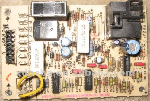
We can prvide a package of service:
· 1. PCB layout, PCB design;
· 2: Make high difficulty PCB(1 to 38 layers)
· 3: Provide all Electronic components;
· 4: PCB assembly;
· 5: Write programs for clients;
· 6: PCBA/finished product Test.
· etc…
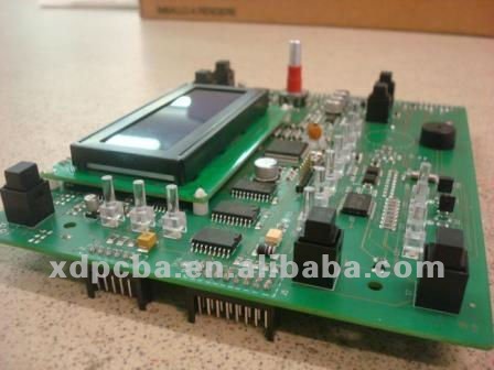
Specification for PCB Manufacture:
Item | Specification |
Numbr of Layer | 1-38Layers |
Material | FR-4,FR2.Taconic,Rogers, CEM-1 CEM-3,ceramic , crockery |
Metal-backed Laminate | |
Remarks | High Tg CCL Is Availabe(Tg>=170ºC) |
Finish Board Thickness | 0.2mm-6.00 mm(8mil-126mil) |
Minimun Core Thickness | 0.075mm(3mil) |
Copper Thickness | 1/2 oz min;12 oz max |
Min.Trace Width & Line Spacing | 0.075mm/0.1mm(3mil/4mil) |
Min.Hole Diameter for CNC Driling | 0.1mm(4mil) |
Min.Hole Diameter for punching | 0.9mm(35mil) |
Biggest panel size | 610mm*508mm |
Hole Positon | +/-0.075mm(3mil) CNC Driling |
Conductor Width(W) | +/-0.05mm(2mil)or |
+/-20% of original artwork | |
Hole Diameter(H) | PTH L:+/-0.075mm(3mil) |
Non-PTH L:+/-0.05mm(2mil) | |
Outline Tolerance | +/-0.125mm(5mil) CNC Routing |
+/-0.15mm(6mil) by Punching | |
Warp & Twist | 0.70% |
Insulation Resistance | 10Kohm-20Mohm |
Conductivity | <50ohm |
Test Voltage | 10-300V |
Panel Size | 110×100mm(min) |
660×600mm(max) | |
Layer-layer misregistration | 4 layers:0.15mm(6mil)max |
6 layers:0.25mm(10mil)max | |
Min.spacing between hole edge to circuity pqttern of an inner layer | 0.25mm(10mil) |
Min.spacing between board oulineto circuitry pattern of an inner layer | 0.25mm(10mil) |
Board thickness tolerance | 4 layers:+/-0.13mm(5mil) |
6 layers:+/-0.15mm(6mil) | |
Impedance Control | +/-10% |
Different Impendance | +-/10% |
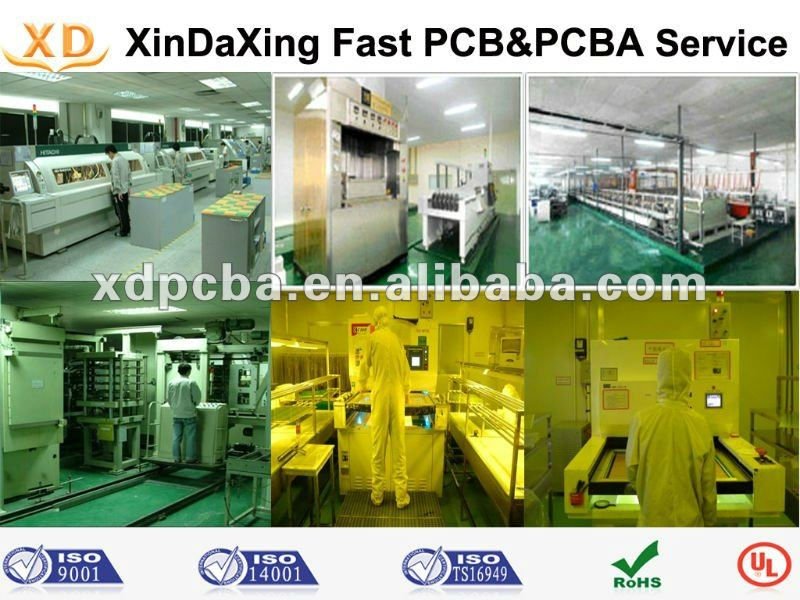
Detailed terms for PCB Assembly
Technical requirement
1)Professional surface-mounting and Through-hole soldering technology
2)Various sizes like 1206,0805,0603 components SMT technology
3)ICT (In Circuit Test),FCT (Functional Circuit Test ) technology
4)PCB Assembly with VL.CE.FCC.Rohs Approval
5)Nitrogen gas reflow soldering technology for SMT
6)High standard SMT&Solder Assembly Line
7)High density interconnected board place ment technology capacity

Quote requirement
1)genber file and Bom list
2)clear pics of PCBA or PCBA Sample for us
3)Test Method for PCBA
Our majoy customers:

 Angle position sensor carbon printing pcb carbon circuit board batch PCB printed circuit board
 Single-sided quartz glass substrate Alumina Ceramic PCBs Biomedical testing 3D printer insulation bed, ceramic substrate luminous keyboard motherboard, alumina pcb grating gear
 High frequency and high speed circuit substrate ceramic pcb Characteristic impedance 50Ω ceramic printed circuit board differential impedance 100Ω ceramic substrate pcb circuit board
 1.0mm Ceramic Circuit Board ENIG alumina circuit board High frequency and high speed printed circuit board ceramic pcb board