


New and Original Voltage Level Translator NLSV2T244MUTAG
- Model Number:NLSV2T244MUTAG
- Type:microcontroller, Microcontroller
- Place of Origin:China
- Brand Name:Original
- D/C:Newest
- Package:Reel
- Brand:Translator
- Voltage - Supply (Vcc/Vdd):0.9V-4.5V
- Voltage - Supply:0.9V-4.5V
- Package / Case:UDFN
- Packing:New*original Packing
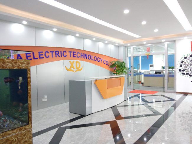
Welcome to XingDa Electric Technology Co.,Ltd
Xindaxing Electric Technology Co.,LTd
Parameters:
| Item | Value |
| Power supply voltage | 0.9V-4.5V |
| Operating temperature | -40--85 |
| Packing | 3K/reel |
| Unit Weight | 0.9KG |
| Product Type | Translation - Voltage Levels |
| Brand | Original |
| Termination type | SMD/SMT |
| Datasheet | Available |
One-stop OEM ODM PCBA manufacturer
We are professional manufacturer in various PCB and PCBA with many 10 experience,We can provide a reasonable price with high quality products.
Our Services
We can provide one-stop service:
1. PCB circuit boards.
2. E-test.
3.Electronic components purchasing.
4. PCB assembly: available on SMT, BGA, DIP.
5. PCBA function test.
6. Enclosure assembly.
Specification for PCB Manufacture:
Item | Specification |
Numbr of Layer | 1-38Layers |
Material | FR-4,FR2.Taconic,Rogers, CEM-1 CEM-3,ceramic , crockery |
Metal-backed Laminate | |
Remarks | High Tg CCL Is Availabe(Tg>=170ºC) |
Finish Board Thickness | 0.2mm-6.00 mm(8mil-126mil) |
Minimun Core Thickness | 0.075mm(3mil) |
Copper Thickness | 1/2 oz min;12 oz max |
Min.Trace Width & Line Spacing | 0.075mm/0.1mm(3mil/4mil) |
Min.Hole Diameter for CNC Driling | 0.1mm(4mil) |
Min.Hole Diameter for punching | 0.9mm(35mil) |
Biggest panel size | 610mm*508mm |
Hole Positon | +/-0.075mm(3mil) CNC Driling |
Conductor Width(W) | +/-0.05mm(2mil)or |
+/-20% of original artwork | |
Hole Diameter(H) | PTH L:+/-0.075mm(3mil) |
Non-PTH L:+/-0.05mm(2mil) | |
Outline Tolerance | +/-0.125mm(5mil) CNC Routing |
+/-0.15mm(6mil) by Punching | |
Warp & Twist | 0.70% |
Insulation Resistance | 10Kohm-20Mohm |
Conductivity | <50ohm |
Test Voltage | 10-300V |
Panel Size | 110×100mm(min) |
660×600mm(max) | |
Layer-layer misregistration | 4 layers:0.15mm(6mil)max |
6 layers:0.25mm(10mil)max | |
Min.spacing between hole edge to circuity pqttern of an inner layer | 0.25mm(10mil) |
Min.spacing between board oulineto circuitry pattern of an inner layer | 0.25mm(10mil) |
Board thickness tolerance | 4 layers:+/-0.13mm(5mil) |
6 layers:+/-0.15mm(6mil) | |
Impedance Control | +/-10% |
Different Impendance | +-/10% |
Technical
1).Professional surface mounting and through hole soldering technology;
2).Various sizes,like 1206,0805,0603,0402,0201 components SMT technology;
3).X-ray ICT(In Circuit Test),FCT(Functional Circuit Test) technology;
4).Nitrogen gas reflow soldering technology for SMT;
5).High standard SMT&Solder Assembly line;
6).High density interconnected board placement technology capacity.
Related Products
10 years focus on high quality PCB, FPC and PCBA!
Company Information
XingDa Electric Technology Co.,Ltd.,is located in Shenzhen, was established in
2011 with more than 200 employees, is a professional manufacturer of PCB, FPC
and PCBA(PCB+components+assembly).
View of Factory
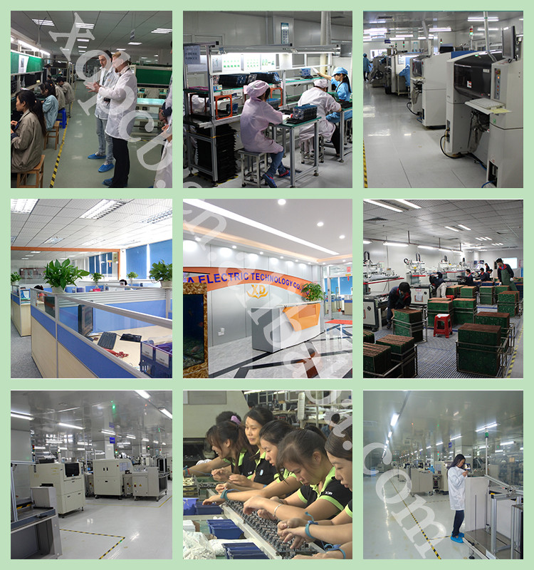
Customer visiting

Exhibition Show:

FAQ
How to work with us?
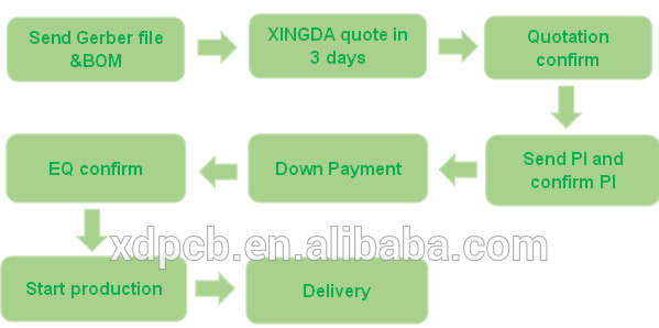
Q1:Are you a factory or trade company?
A: XingDa is a PCB/FPC/PCBA manufacturer/factory. We pecialize in PCB/PCBs Board for 6 years.
Q2:Is my PCB file safe if I send it to you for manufacturing?
A: We respect customer's design authority and will never manufacture PCB for someone else without your permission. NDA is acceptable.
Q3:Can you copy PCB samples without Gerber file?
A: Yes, we can clone the PCB according to your samples.
Q4:What payment do you accept ?
A: TT/ Western Union/ Paypal/
Q5: What's your shipping way ?
A: 1. We have our own forwarder to ship goods by DHL, UPS, FEDEX, TNT,EMS.
2. If you have your own forwarder, we can cooperate with them.
Q6: How about the MOQ?
A: For PCB: 1 pcs
For PCBA: 1000pcs
Q7: What's your main market?
A:Europe, USA, Brazil, Russia, Turkey, Iran, Austrialia, Singapore...
Packaging & Shipping

Specification for PCB Manufacture:
Item | Specification |
Numbr of Layer | 1-38Layers |
Material | FR-4,FR2.Taconic,Rogers, CEM-1 CEM-3,ceramic , crockery |
Metal-backed Laminate | |
Remarks | High Tg CCL Is Availabe(Tg>=170ºC) |
Finish Board Thickness | 0.2mm-6.00 mm(8mil-126mil) |
Minimun Core Thickness | 0.075mm(3mil) |
Copper Thickness | 1/2 oz min;12 oz max |
Min.Trace Width & Line Spacing | 0.075mm/0.1mm(3mil/4mil) |
Min.Hole Diameter for CNC Driling | 0.1mm(4mil) |
Min.Hole Diameter for punching | 0.9mm(35mil) |
Biggest panel size | 610mm*508mm |
Hole Positon | +/-0.075mm(3mil) CNC Driling |
Conductor Width(W) | +/-0.05mm(2mil)or |
+/-20% of original artwork | |
Hole Diameter(H) | PTH L:+/-0.075mm(3mil) |
Non-PTH L:+/-0.05mm(2mil) | |
Outline Tolerance | +/-0.125mm(5mil) CNC Routing |
+/-0.15mm(6mil) by Punching | |
Warp & Twist | 0.70% |
Insulation Resistance | 10Kohm-20Mohm |
Conductivity | <50ohm |
Test Voltage | 10-300V |
Panel Size | 110×100mm(min) |
660×600mm(max) | |
Layer-layer misregistration | 4 layers:0.15mm(6mil)max |
6 layers:0.25mm(10mil)max | |
Min.spacing between hole edge to circuity pqttern of an inner layer | 0.25mm(10mil) |
Min.spacing between board oulineto circuitry pattern of an inner layer | 0.25mm(10mil) |
Board thickness tolerance | 4 layers:+/-0.13mm(5mil) |
6 layers:+/-0.15mm(6mil) | |
Impedance Control | +/-10% |
Different Impendance | +-/10% |


