
Related Article
Introduction:
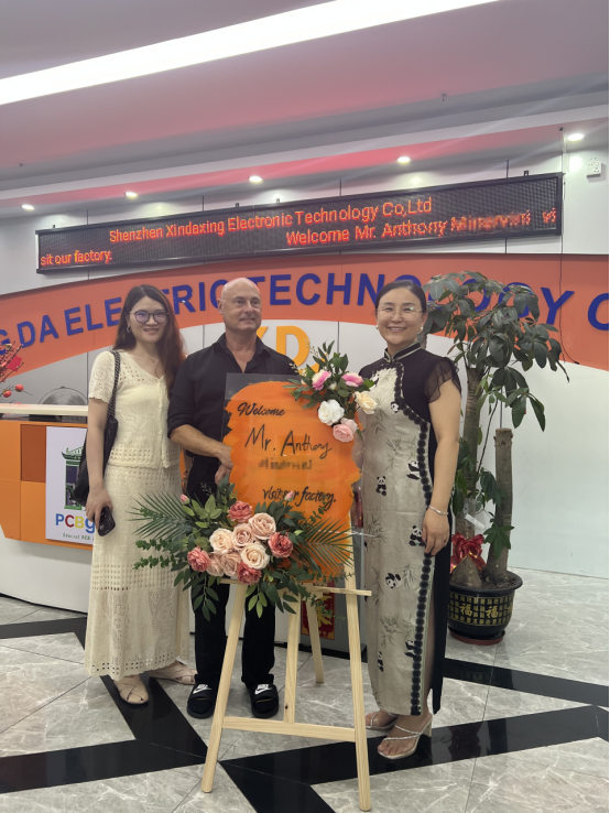
Recently,Anthony, from America who belongs to the well-known optical microphone industry visited our PCBA factory to field investigation and technical exchange. The purpose of this visit is to further deepen the cooperation between the two sides and jointly explore the future innovative development direction of the microphone industry.
Recently,Anthony, from America who belongs to the well-known optical microphone industry visited our PCBA factory to field investigation and technical exchange. The purpose of this visit is to further deepen the cooperation between the two sides and jointly explore the future innovative development direction of the microphone industry.
Anthony visited PCBA factory:Deepen cooperation

"Hot spots" high-end printed circuit board gap between supply and demand to expand; Many PCB companies included in the blockbuster list... 01.According to DIGITIMES, recently used in server and data center of the high-end PCB demand, especially ABF loading board (FC - BGA) out of stock...
High-end Printed Circuit Board Gap Between Supply And Demand To Expand; Many PCB Companies Included in The Blockbuster List
As a listed company of Foxconn, Pengding Holdings (002938) continues to maintain a leading position in the world From 2017 to 2020, the operating revenue of Pengding Holdings (002938.SZ) increased from 23.921 billion yuan to 29.851 billion yuan. According to the statistics of some...
S A Listed Company Of Foxconn, Pengding Holdings (002938) Continues To Maintain A Leading Position in The World
PCB manufacturing analysis In PCB manufacturing process, may involve several participants, from the designer to the developers, project director, sales, business development, personnel, financial personnel, government officials and industry associations. How to ensure that all the participants...
PCB Manufacturing Analysis