


Smart ring with an ultra-thin six-layer rigid flex PCB polyimide pcb without NFC wireless charging flex pcb
pcbgate251122143
Product Definition: Intelligent Ring Ultra-thin Six-layer Soft-Hard Hybrid Substrate: It is an ultra-thin basic circuit board for intelligent ring electronic devices. It combines the advantages of soft boards and hard boards to achieve better performance and functions. This combined board usually consists of six layers, each with its specific function and role. The design of ODM and OEM manufacturing of the intelligent ring ultra-thin six-layer soft-hard hybrid board needs to take into account multiple aspects such as the structure of the device, ID size, power consumption, weight, durability, heat dissipation performance, and electromagnetic shielding performance, to ensure that the device can meet the needs of users and has a longer service life.
Product features and highlights: Due to the limited space of the smart ring, the soft and hard composite board must be extremely thin. The connection area between the local hard board sections and the local soft board sections is very narrow, which poses a considerable manufacturing challenge.
Product Applications: Bluetooth hard networking smart ring, health monitoring smart ring, sports monitoring smart ring
Product features and highlights: Due to the limited space of the smart ring, the soft and hard composite board must be extremely thin. The connection area between the local hard board sections and the local soft board sections is very narrow, which poses a considerable manufacturing challenge.
Product Applications: Bluetooth hard networking smart ring, health monitoring smart ring, sports monitoring smart ring
Quantity:
1.00
Unable to ship to shipping address, please feedback to us
Smart ring with an ultra-thin six-layer rigid flex PCB polyimide pcb without NFC wireless charging flex pcb

Specifications:
Product hole: Minimum metallization hole diameter: (0.1 ± 0.05); Minimum non-metallization hole diameter
None Product line: Minimum line width: 0.11 ± 0.02 mm Minimum line spacing: 0.055 ± 0.02 mm
Product solder mask & characters: Solder mask window size: 0.7 ± 0.075 mm Character silk-screen line width: 0.125 mm
Finished product related dimensions: 62.6 * 7.3 mm Surface treatment: Gold plating 1-2 layers
Functional testing: Flying probe test, incomplete scanning of circuit AOI Reliability test: Thermal shock test, Tin plating test
Product solder mask & characters: Solder mask window size: 0.7 ± 0.075 mm Character silk-screen line width: 0.125 mm
Finished product related dimensions: 62.6 * 7.3 mm Surface treatment: Gold plating 1-2 layers
Functional testing: Flying probe test, incomplete scanning of circuit AOI Reliability test: Thermal shock test, Tin plating test
--Written by Lisa-25.11.20

PCB product Capacity
| Value | Specification |
PCB Max. size | 510mm*1200mm(SMT) |
| Remarks | High Tg CCL is Available(Tg>=180℃) |
| Finish Board Thickness | 0.2 mm-6.00mm(8mil-126mil) |
| Surface Finish | Gold finger(>=0.13um), Immersion Gold(0.025-0075um), Plating Gold(0.025-3.0um), HASL(5-20um), OSP(0.2-0.5um) |
| Shape | Routing、Punch、V-cut、Chamfer |
| Surface Treatment | Solder Mask(black, green, white, red, blue, thickness>=12um, Block, BGA) |
| Silkscreen(black, yellow, white) | |
| Peel able-mask(red, blue, thickness>=300um) | |
| Minimum Core | 0.075mm(3mil) |
| Copper Thickness | 1/2 oz min; 12oz max |
| Min Trace Width & Line Spacing | 0.075mm/0.1mm(3mil/4mil) |
| Min Hole Diameter for CNC Drilling | 0.1mm(4mil) |
| Min Hole Diameter for Punching | 0.6mm(35mil) |
| Biggest panel size | 610mm * 508mm |
| Hole Position | +/-0.075mm(3mil) CNC Drilling |
| Conductor Width(W) | +/-0.05mm(2mil) or +/-20% of original |
| Hole Diameter(H) | PTHL:+/-0.075mm(3mil) |
| Non PTHL:+/-0.05mm(2mil) | |
| Outline Tolerance | +/-0.1mm(5mil) CNC Routing |
| Warp & Twist | 0.70% |
| Insulation Resistance | 10Kohm-20Mohm |
| Conductivity | <50ohm |
| Test Voltage | 10-300V |
| Panel Size | 110 x 100mm(min) |
| 660 x 600mm(max) | |
| Layer-layer misregistration | 4 layers:0.15mm(6mil)max |
| 6 layers:0.25mm(10mil)max | |
| Min spacing between hole edge to circuitry pattern of an inner layer | 0.25mm(10mil) |
| Min spacing between board outline to circuitry pattern of an inner layer | 0.25mm(10mil) |
| Board thickness tolerance | 4 layers:+/-0.13mm(5mil) |
Flexible PCB product Capacity
| Value | Capabilities |
| Items | FR-4, FR1,FR2; CEM-1, CEM-3,Rogers,Teflon,Arlon,Aluminum Base, Copper Base,Ceramic, Crockery, etc. |
| Layers | FPC:1 to 6 Layers,Rigid Flex:2 to 10 Layers |
| Base Copper Thickness | 1/3 oz to 2oz |
| Regular Base Material Thickness | 12.5um to 50um(FPC) |
| 0.1mm to 3.2mm(Rigid) | |
| Regular Coverlay Thickness | 27um to 50um |
| Regular Adhesive Thickness | 12um to 25um |
| Blind or Buried Vias | Yes |
| Impedance Control | Yes |
| Min.Line Width/Spacing | 0.04mm/0.04mm |
| Surface Finishing | Electroplate Ni/Au(Flash gold/Soft gold/Hard gold),ENIG,Immersion Tin; plated silver;immersion silver ; OSP,HASL |
| Outline Fabrication | Die cut,laser cut,CNC routing,V-scoring |
| Hole to edge(Hard tool/Die Cut) | ±0.1/±0.2mm |
| Edge to edge(Hard tool/Die Cut) | ±0.05/±0.2mm |
| Circuit to edge(Hard tool/Die Cut) | ±0.07/±0.2mm |
PCB Assembly(SMT) Product Capacity
| Value | SMT Capacity |
| PCB Max. size | 510mm*1200mm(SMT) |
| Chip component | 01005,0201, 0402, 0603, 0805, 1206 package |
| Min.pin space of IC | 0.1mm |
| Min. space of BGA | 0.1mm |
| Max.precision of IC assembly | ±0.01mm |
| Surface Treatment | ≥8 million pionts/day |
| 6 DIP production lines | |
| Assembly testing | Current test, voltage test, high temperature and low temperature test. |
| Drop Impact Test,aging test,water proof test,leakage-proof test and etc. | |
| Different test can be done according to your requirement. |

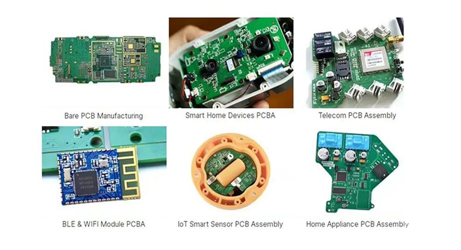
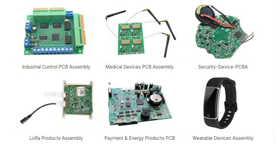
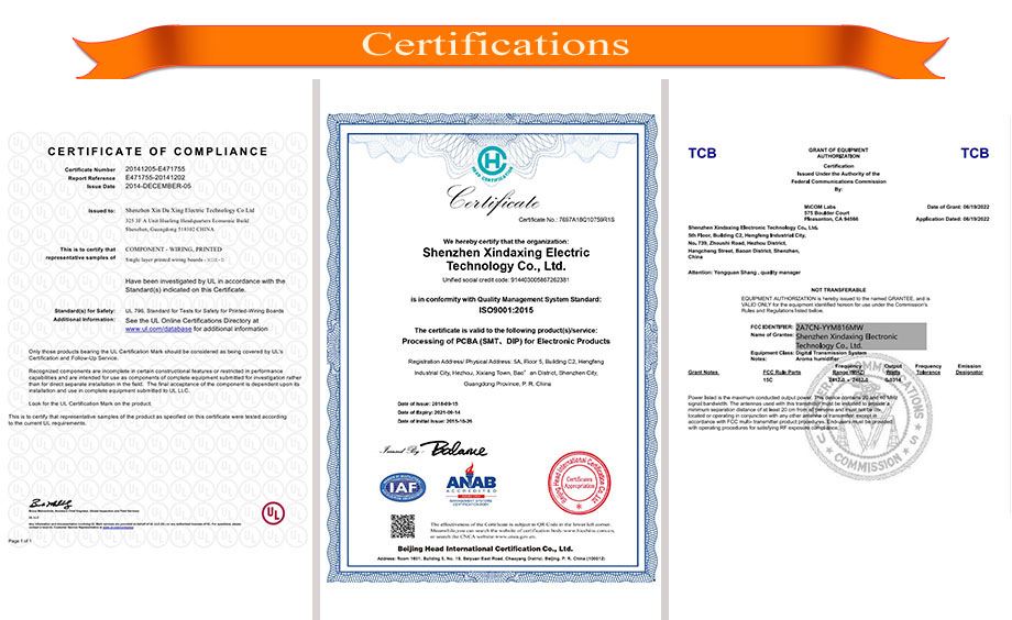
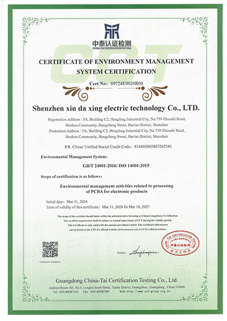
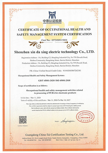
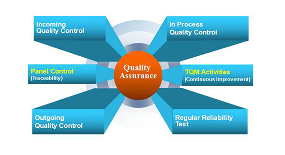
Quality Control
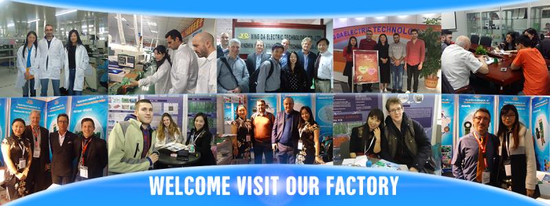
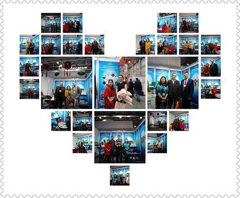
Customers Visit our factory
Exhibition Show
Munich Exhibition&Moscow:

Russia Exhibition:


Q1:Are you a factory or trade company?
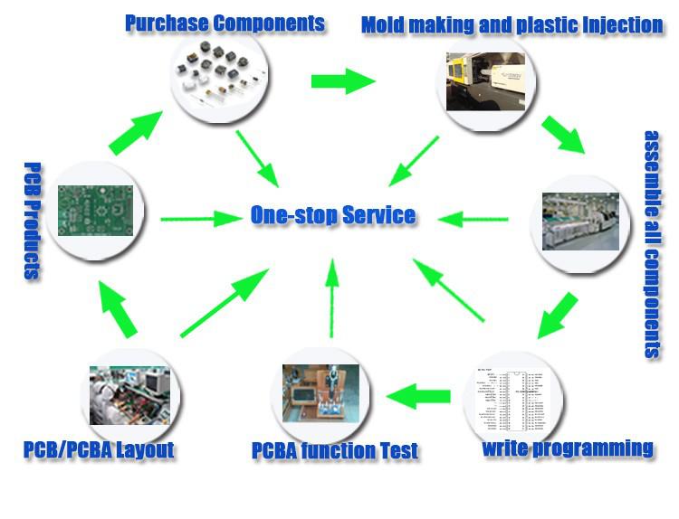
A: Xing Da Electronic Technology Co., ltd is leading OEM PCB&PCBA manufacturer in China with over 14 years rich experience. Our aim is “One-Stop service, smart manufacturing, make your production easier.”
Q2: What is needed for quotation?
A:1. PCB&FPC
We need Gerber files and specification for quotation
2. PCBA (= PCBA+ components + Assembly)
For PCBA, please send Gerber files, specification and Bom list for factory price.
A: Xing Da Electronic Technology Co., ltd is leading OEM PCB&PCBA manufacturer in China with over 14 years rich experience. Our aim is “One-Stop service, smart manufacturing, make your production easier.”
Q2: What is needed for quotation?
A:1. PCB&FPC
We need Gerber files and specification for quotation
2. PCBA (= PCBA+ components + Assembly)
For PCBA, please send Gerber files, specification and Bom list for factory price.
Q3:Is my PCB or PCBA files safe if I send it to you for manufacturing?
A: We respect customer's design authority and will never manufacture PCB or PCBA for someone else without your permission. We never share customer documents with third parties.NDA is acceptable.
Q4:What payment do you accept ?
A: T/T,Western Union,Paypal, L/C,Credit Card, Cheque,Others
A: We respect customer's design authority and will never manufacture PCB or PCBA for someone else without your permission. We never share customer documents with third parties.NDA is acceptable.
Q4:What payment do you accept ?
A: T/T,Western Union,Paypal, L/C,Credit Card, Cheque,Others
Q5: What's your shipping method?
A: 1. We have our own forwarders to ship goods with competitive price by DHL, UPS, FEDEX, TNT,EMS etc. We can also arrange shipments via sea or air depending on your specific requirements."
2. If you have your own forwarder, we can cooperate with them.
Q6: How about the MOQ?
A: There is no MOQ. We can produce prototypes, small orders, or large volumes.
A: 1. We have our own forwarders to ship goods with competitive price by DHL, UPS, FEDEX, TNT,EMS etc. We can also arrange shipments via sea or air depending on your specific requirements."
2. If you have your own forwarder, we can cooperate with them.
Q6: How about the MOQ?
A: There is no MOQ. We can produce prototypes, small orders, or large volumes.


