


High Density ENIG Multilayer FR4 PCB Board
High Density ENIG Multilayer FR4 PCB Board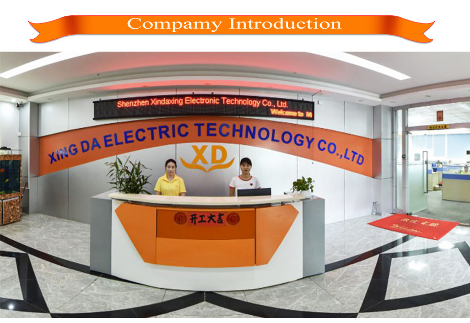
Shenzhen Xin Da Xing Electric Technology Co., Ltd was founded in September 2011, our company is a professional PCB manufacturing, sales and service enterprise, also provide customers with complete BOM list procurement services.
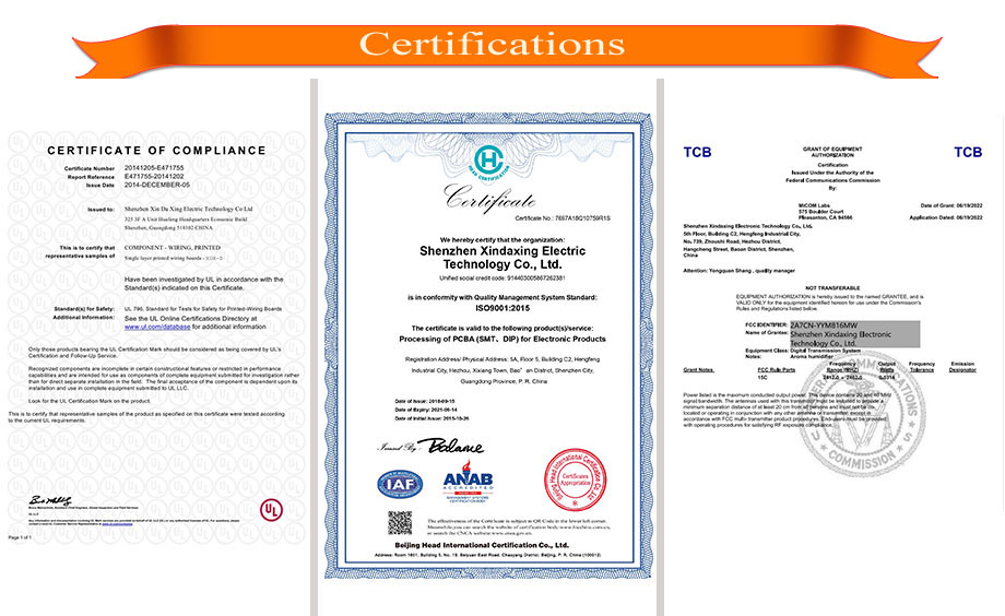
We have got certification of ISO 9001 and UL. Our capacity including: 1-32 layers FR4 PCB board manufacturing, 1-6 layers Flexible PCB manufacturing, Aluminum PCB, Ceramic PCB and Carbon PCB manufacturing. Monthly production capacity ismore than 50,000 square meter.
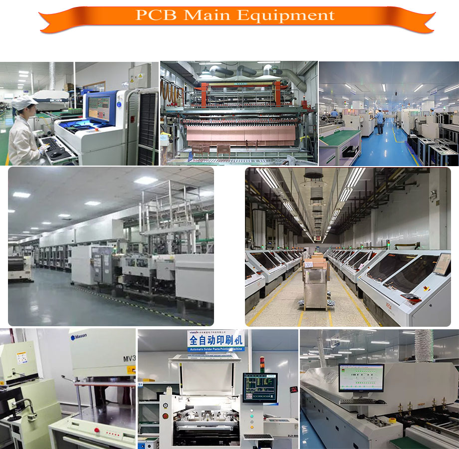
The company has introduced advanced automation equipment and production technology, trained a number of innovative, skilled professionals, with high-end product structure, professional product manufacturing technology, stable quality performance and well management system, Xing Da has established long-term and stable cooperate relations with the world's leading communication equipment, medical equipment, aerospace electronics, automotive electronics, home appliances manufacturers.
Xing Da provides customers with high-quality products and services, is committed to becoming the most respected enterprise. Aspire to become a world-class PCB supplier and best quality electronic components supplier.
Specification
Layer: 4 layers
Material: FR-4
Copper Thickness (in OZ): 1OZ
Finish Board Thickness: 1.6 mm
Solder Mask: Green
Silkscreen: White
Surface Finish: HASL
Minimum aperture: 0.015mm
Minimum line spacing: 0.065mm
Minimum line width: 0.065

| Value | Specification |
| Material | FR-4,FR1, CEM-1, CEM-3,Aluminum, Ceramic, Metal-backed Laminate, etc. Also make Crockery, Taconic, Rogers PCBs etc. |
| Remarks | High Tg CCL is Available(Tg>=170℃) |
| Finish Board Thickness | 0.2 mm-6.00mm(8mil-126mil) |
| Surface Finish | Gold finger(>=0.13um), Immersion Gold(0.025-0075um), Plating Gold(0.025-3.0um), HASL(5-20um), OSP(0.2-0.5um) |
| Shape | Routing、Punch、V-cut、Chamfer |
| Surface Treatment | Solder Mask(black, green, white, red, blue, thickness>=12um, Block, BGA) |
| Silkscreen(black, yellow, white) | |
| Peel able-mask(red, blue, thickness>=300um) | |
| Minimum Core | 0.075mm(3mil) |
| Copper Thickness | 1/2 oz min; 12oz max |
| Min Trace Width & Line Spacing | 0.075mm/0.1mm(3mil/4mil) |
| Min Hole Diameter for CNC Drilling | 0.1mm(4mil) |
| Min Hole Diameter for Punching | 0.6mm(35mil) |
| Biggest panel size | 610mm * 508mm |
| Hole Position | +/-0.075mm(3mil) CNC Drilling |
| Conductor Width(W) | +/-0.05mm(2mil) or +/-20% of original |
| Hole Diameter(H) | PTHL:+/-0.075mm(3mil) |
| Non PTHL:+/-0.05mm(2mil) | |
| Outline Tolerance | +/-0.1mm(5mil) CNC Routing |
| Warp & Twist | 0.70% |
| Insulation Resistance | 10Kohm-20Mohm |
| Conductivity | <50ohm |
| Test Voltage | 10-300V |
| Panel Size | 110 x 100mm(min) |
| 660 x 600mm(max) | |
| Layer-layer misregistration | 4 layers:0.15mm(6mil)max |
| 6 layers:0.25mm(10mil)max | |
| Min spacing between hole edge to circuitry pattern of an inner layer | 0.25mm(10mil) |
| Min spacing between board outline to circuitry pattern of an inner layer | 0.25mm(10mil) |
| Board thickness tolerance | 4 layers:+/-0.13mm(5mil) |
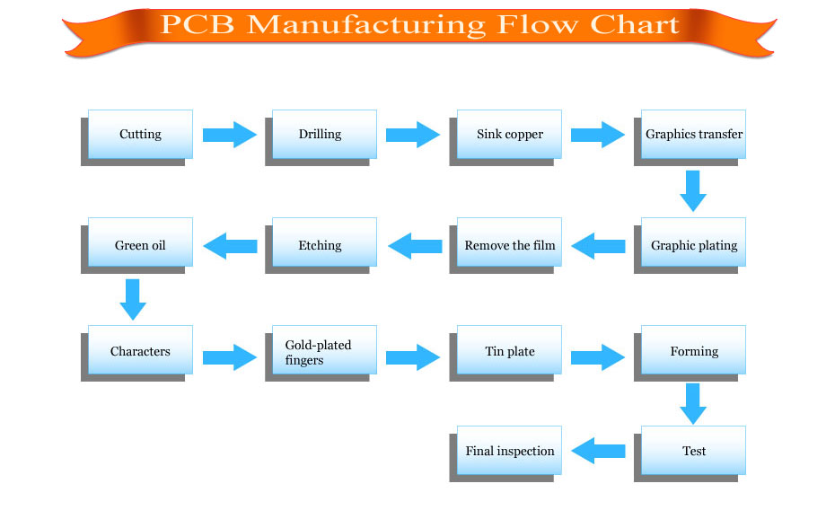


Q1.For PCB quotation what files format does Xing Da need?
A:Gerber, Protel 99SE, DXP, PADS 9.5, AUTOCAD, CAM350 are OK.
Q2.MOQ and what is Xing Da fastest delivery time?
A:1pcs. Sample to mass production all can be supported by Xing Da.
Q3.How to test PCB boards?
A:AOl, Fly probe testing, Text fixture testing, FOC etc. for bare PCB.
Q4.Can you do PCB or circuit design?
A:Yes,we have design team including software, hardware and structure engineers.
We can supply customized design service. Give your idea and we can make it true.
Q5.Which payment terms does Xing Da accept?
A:T/T, Western Union, PayPal, Money Gram and so on.


