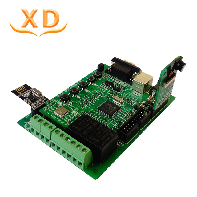
PCBA manufacturing pcba with DIP components soldering circuit boards
PCBA manufacturing pcba with DIP components soldering circuit boards
What is Dip Soldering?
Dip soldering is a manufacturing process where a technician dips objects into a bath of molten solder to fix parts together. The most common application of this technique is in the production of circuit boards, where it can be a fast and efficient method. The heat of the solder can potentially damage parts of the project, and the technician has to make sure all the components can take the heat before dipping; usually the project is all metal to avoid this problem.
With circuit board production, the solder will stick to the exposed mental components and will not adhere to areas without metal or areas treated with a chemical to resist solder. Dip soldering may be a hand operation, with a technician personally dipping the product, and it is also possible to partially automate it. A machine can grip the circuit board, dip it at the right angle, and keep it in the solder for the correct period of time before pulling it out.
The dip soldering process is similar to wave soldering, a mass production process people use to make chips. With wave soldering, it is all automated, and the chips pass under a steady flow of melted solder material, rather than being dipped. This process costs more money to implement and allows people to produce more projects per day, making it suitable for large scale facilities where people need to cut down on manufacturing time.
For small-scale soldering, dip soldering can be a useful technique. People do not need very much equipment to set it up, simply a container large enough to dip projects, with appropriate tools for melting the solder so it will be usable. Many companies manufacture the necessary supplies, and people can also make their own. For automated setups, slightly larger investments are needed to purchase a machine capable of handling the process.
People may learn this and other techniques on the job or while in a training program to prepare for a professional career. There are a number of types of solder available, and the technician has to be able to choose the correct mixture and make other decisions during the process to make sure the final product will perform properly. People usually inspect the project after dip soldering to see if any manual adjustments are necessary, such as cleaning excess solder off a contact or discarding an item with damage like pockmarks or distortions from the soldering process.
Overview
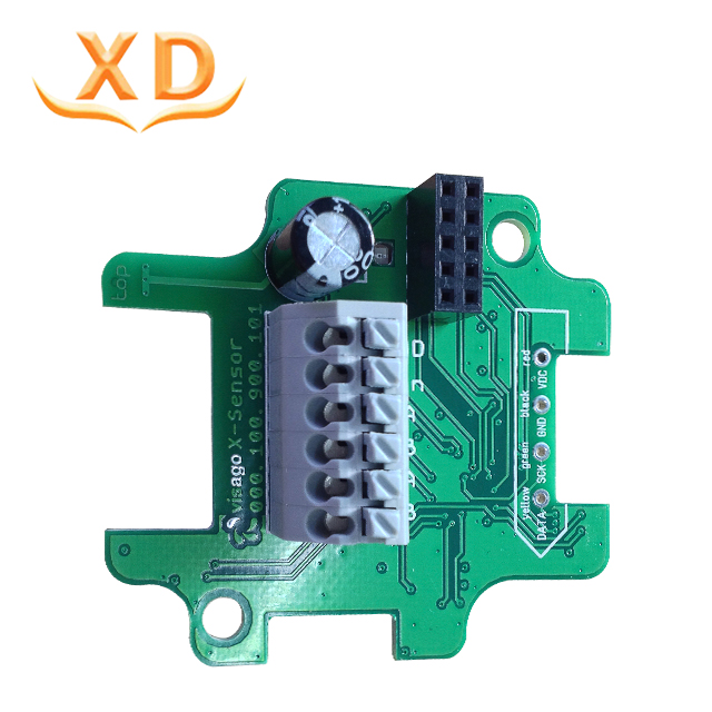
Xinda provides PCBA assembly, low to medium MASS production volume. Our professional SMT factory has advanced equipment, such as the world-class stencil printing, SMT chip pick & place, solder reflow, and in-line testing and steel mesh manufacturing. AOI test machine and X-ray testing machines for quality check.Xinda PCB Assembly
Xinda offers turn-key PCB assembly services OEM in prototype quantities or low-volume to mid-volume production runs. We handle the whole process including: ordering all the components, PCB manufacturing, PCB assembly, testing and final shipment. We are capable of assembling BGA, Micro-BGA, QFN and other leadless package parts.
| SMT and Through-Hole Assembly | Fine Pitch Component Insertion |
| Lead free Assembly | BGA and QFN Assembly |
| One-stop PCB Assembly | BGA X-Ray Inspection |
| Prototype PCB Assembly | Automated Optical Inspection |
| PCB Assembly in low volumes | PCB testing for functionality |
| AOI Testing Checks for solder paste Checks for components down to 0201" Checks for missing components, offset, incorrect parts, polarity X-Ray Inspection X-Ray provides high-resolution inspection | In-Circuit Testing In-Circuit Testing is commonly used in conjunction with AOI minimizing functional defects caused by component problems. Power-up Test Advanced Function Test Flash Device Programming Functional testing |
| Selective Wave Soldering | Conformal Coating |
| Complete box build | Kitting and 3D printing |
Surface Mount Technology Xinda all products follow IPC2 standards.With 18 years experience of placing BGA, UBGA, CSP and small profile passives down to and including 0201, Xinda offers a cost effective high yield solution to any SMT requirement. Pin Through Hole Capabilities to place tape and reeled radial components sizes. Maximum PCB size is 40"x 40". Placement rates reach 15000 pieces per hour with an accuracy of 99% minimizing component loss. RoHS Regulations Xinda have 2 kinds of solutions. Leadfree and leaded soldering process. Each solutions room are divided into 2 seperated places. so there is no mix up. Selective Wave Solder Having the Selective Wave soldering machines, Xinda achieves consistent quality and process control when assembling boards having multiple ground and power planes, high-current connectors or A-typical distribution of components. All AOI tested before QC.IPQC. Conformal coating Both dip-coating and vertical spray coating is available. Protecting non conductive dielectric layer that is applied onto the printed circuit board assembly to protect the electronic assembly from damage due to contamination, salt spray, moisture, fungus, dust and corrosion caused by harsh or extreme environments. When coated, it is clearly visible as a clear and shiny material. |
Company Information
XingDa Electric Technology Co.,Ltd.,is located in Shenzhen, was established in
2011 with more than 200 employees, is a professional manufacturer of PCB, FPC
and PCBA(PCB+components+assembly).
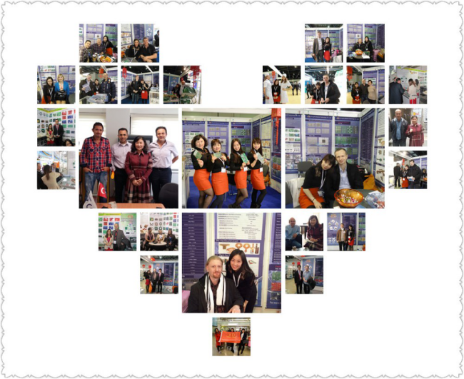
Exhibition Show:
FAQ
Q1:Are you a factory or trade company?
A: XingDa is a PCB/FPC/PCBA manufacturer/factory. We pecialize in PCB/PCBs Board for 6 years.
Q2:Is my PCB file safe if I send it to you for manufacturing?
A: We respect customer's design authority and will never manufacture PCB for someone else without your permission. NDA is acceptable.
Q3:Can you copy PCB samples without Gerber file?
A: Yes, we can clone the PCB according to your samples.
Q4:What payment do you accept ?
A: TT/ Western Union/ Paypal/
Q5: What's your shipping way ?
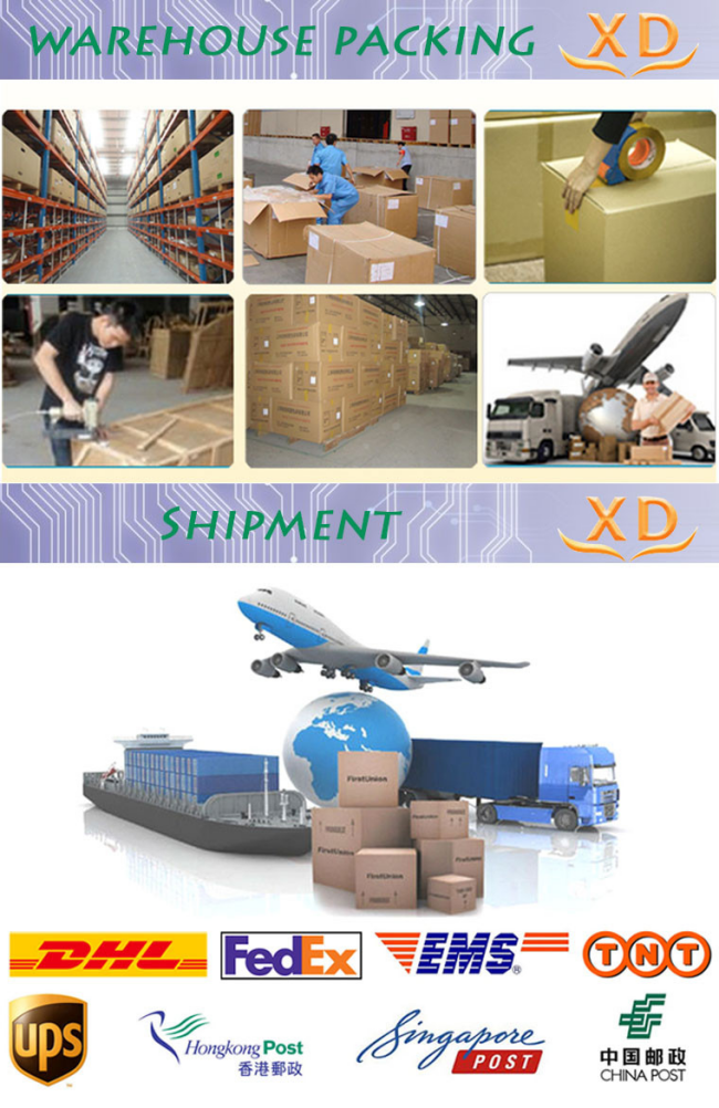
A: 1. We have our own forwarder to ship goods by DHL, UPS, FEDEX, TNT,EMS.
2. If you have your own forwarder, we can cooperate with them.
Q6: How about the MOQ?
A: For PCB: 1 pcs
For PCBA: 1000pcs
Q7: What's your main market?
A:Europe, USA, Brazil, Russia, Turkey, , Austrialia, Singapore...
Packaging & Shipping