


HDI bare board prototype board
PCB-8
The process of performing electrical testing on an unassembled PCB is called bare board testing. In PCB assembly prototyping, bare-board testing helps ensure potential problems are discovered before components are assembled.
Quantity:
0.00
Unable to ship to shipping address, please feedback to us
products/hdi-bare-board-prototype-board.html
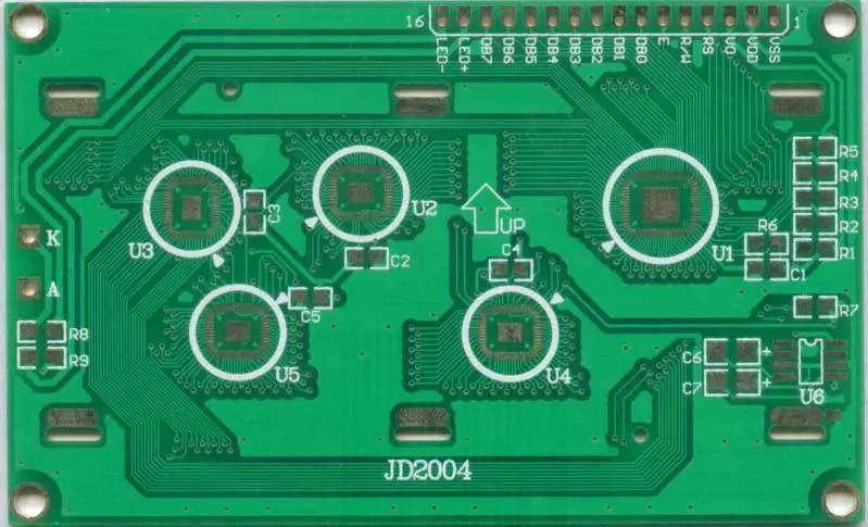
What is the use of a bare PCB board?
The bare PCB board is the skeleton of the traditional circuit board. It directs current and current through appropriate paths and is used in most computing electronics.
The simplicity of a blank PCB gives engineers and designers enough freedom to add components as needed. This blank board provides flexibility and enables mass production.
This PCB board requires more design work than other routing methods, but can often be automated after assembly and fabrication. This makes PCB boards the cheapest and most efficient option.
Bare boards are only useful when components are added. The ultimate purpose of a bare PCB is to be a complete circuit board, which can have a variety of uses if matched with the right components.
However, this is not the only use of bare PCB boards. A blank PCB is the best stage in the circuit board manufacturing process to perform bare board testing. It is essential to prevent many problems that may arise later.
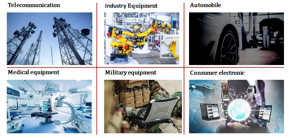
Application
Products are widely used in Telecommunications, Computing networks, Medical equipment,
Automobile and other high-tech fields
What is the use of a bare PCB board?
The bare PCB board is the skeleton of the traditional circuit board. It directs current and current through appropriate paths and is used in most computing electronics.
The simplicity of a blank PCB gives engineers and designers enough freedom to add components as needed. This blank board provides flexibility and enables mass production.
This PCB board requires more design work than other routing methods, but can often be automated after assembly and fabrication. This makes PCB boards the cheapest and most efficient option.
Bare boards are only useful when components are added. The ultimate purpose of a bare PCB is to be a complete circuit board, which can have a variety of uses if matched with the right components.
However, this is not the only use of bare PCB boards. A blank PCB is the best stage in the circuit board manufacturing process to perform bare board testing. It is essential to prevent many problems that may arise later.
| PCB product Capacity | ||
| PCB Item | Standard | Advanced |
| Layer Counts: | 1L--10L, HDI | 10L-18L,HDI |
| Base Material: | CAM1,FR4,F4BK,Arlon,Rogers | |
| Material Suppliers: | GUOJI(GDM), KINGBOARD(KB), SHENGYI,Arlon,Rogers | |
| Material Thickness(mm): | 0.40, 0.60, 0.80, 1.00, 1.20, 1.50, 1.60, 2.0, 2.4, 3.2 | |
| Max board size(mm): | 1200x400mm | 1200x500mm |
| Board Outline Tolerance: | ±0.15mm | ±0.01mm |
| Board Thickness: | 0.4mm--3.2mm | 0.3mm----3.2mm |
| Thickness Tolerance: | ±5% | ±3% |
| Minimum line/space: | 0.1mm | |
| Mini Hole Size(mechanical): | 0.2mm | |
| Innerlayer Copper Weight: | 0.1mm | |
| Innerlayer Copper Weight: | 17um--105um | |
| Outlayer Copper Weight: | 17um--105um | |
| Mini Solder Mask Bridge: | 0.05mm | |
| Impedance Control Tolerance: | ±10% | |
| Contours: | Scored, Routed, Punched | |
| Surface Finishing: | HAL,lead-free HAL,ENIG,Plated Gold,Immersion Silver,OSP | |
| 1--2L Lead Time: | 2-5 days | |
| 4--18L Lead Time: | 5-10 days | |
| Acceptable File Format: | Gerber file,Powerpcb,CAD,AUTOCAD,ORCAD,P-CAD,CAM-350,CAM2000 | |
| Quality Standards: | IPC-A-600H Class2 | |
Application
Products are widely used in Telecommunications, Computing networks, Medical equipment,
Automobile and other high-tech fields
Recommend Products
 Angle position sensor carbon printing pcb carbon circuit board batch PCB printed circuit board
 Single-sided quartz glass substrate Alumina Ceramic PCBs Biomedical testing 3D printer insulation bed, ceramic substrate luminous keyboard motherboard, alumina pcb grating gear
 High frequency and high speed circuit substrate ceramic pcb Characteristic impedance 50Ω ceramic printed circuit board differential impedance 100Ω ceramic substrate pcb circuit board
 1.0mm Ceramic Circuit Board ENIG alumina circuit board High frequency and high speed printed circuit board ceramic pcb board