


fr4 pcb heavy copper pcb making
PCB-10
Industries that benefit from heavy copper printed circuit boards are military/defense, automotive, solar panel and soldering equipment manufacturers, and other industries that require circuit boards that can handle the heat generated by today's complex electronics.
By cladding copper on the FR4 material, you can get the most commonly used rigid PCB material copper clad laminate, also written as CCL. FR4 CCL is the most widely used substrate for printed circuit board (PCB) manufacturers to make bare PCBs because of its high mechanical value and electrical insulating qualities. For PCBs, the FR4 material only forms the main insulating skeleton. If we want to make double-sided PCB or multi-layer PCB, we need to use FR4 core, prepreg (PP) and copper foil, heat and press them in a laminator to laminate one or more layers after trace etching.
By cladding copper on the FR4 material, you can get the most commonly used rigid PCB material copper clad laminate, also written as CCL. FR4 CCL is the most widely used substrate for printed circuit board (PCB) manufacturers to make bare PCBs because of its high mechanical value and electrical insulating qualities. For PCBs, the FR4 material only forms the main insulating skeleton. If we want to make double-sided PCB or multi-layer PCB, we need to use FR4 core, prepreg (PP) and copper foil, heat and press them in a laminator to laminate one or more layers after trace etching.
Quantity:
0.00
Unable to ship to shipping address, please feedback to us
fr4 pcb heavy copper pcb making
Introduce:
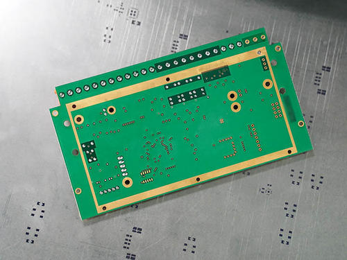
A heavy copper PCB is a printed circuit board with 3 or more ounces of finished copper on the inner and/or outer layers.
While there is no standard definition for heavy copper, it is generally accepted that a printed circuit board is called a heavy copper PCB if 3 ounces (oz) or more of copper is used on the inner and outer layers. Any circuit with a copper thickness greater than 4 ounces per square foot (ft2) is also classified as a thick copper PCB. Extreme copper is 20 ounces per square foot to 200 ounces per square foot.
When electronic devices require high power or current flow, we need to consider using thick copper to control the heat on the PCB
The benefits of heavy copper in PCBs:
reduce thermal strain
better current conductivity
Can withstand repeated thermal cycling
Smaller PCB size due to copper layering
Increase connector site strength
Specification

Packing & Delivery

Introduce:
A heavy copper PCB is a printed circuit board with 3 or more ounces of finished copper on the inner and/or outer layers.
While there is no standard definition for heavy copper, it is generally accepted that a printed circuit board is called a heavy copper PCB if 3 ounces (oz) or more of copper is used on the inner and outer layers. Any circuit with a copper thickness greater than 4 ounces per square foot (ft2) is also classified as a thick copper PCB. Extreme copper is 20 ounces per square foot to 200 ounces per square foot.
When electronic devices require high power or current flow, we need to consider using thick copper to control the heat on the PCB
The benefits of heavy copper in PCBs:
reduce thermal strain
better current conductivity
Can withstand repeated thermal cycling
Smaller PCB size due to copper layering
Increase connector site strength
Specification
| item | value |
| Number of Layers | 12-layer |
| Base Material | FR4 |
| Copper Thickness | 0.5~9OZ |
| Board Thickness | 0.1~7mm |
| Min. Hole Size | 0.075mm |
| Min. Line Width | 2Mil |
| Min. Line Spacing | 2Mil |
| Surface Finishing | HASL Imm Ni/Au, Imm Tin, OSP |
| Product name | Printed Circuit Board |
| Application | Electronics Device |
| Type | Electronic Board |
| Service | PCB+Components+Assembly |
| Soldermask color | White, Black, Blue, Green, Grey, Red, Yellow, Transparent |
| Certificate | IATF16949, ISO, RoHs |
| Layers | 1~32layers |
| Max Panel Size | 800*1200mm |
| Finger(Au) | 1~50U'' |
| Min Half Hole/Slot | 0.3mm |
Packing & Delivery
Recommend Products
 Angle position sensor carbon printing pcb carbon circuit board batch PCB printed circuit board
 Single-sided quartz glass substrate Alumina Ceramic PCBs Biomedical testing 3D printer insulation bed, ceramic substrate luminous keyboard motherboard, alumina pcb grating gear
 High frequency and high speed circuit substrate ceramic pcb Characteristic impedance 50Ω ceramic printed circuit board differential impedance 100Ω ceramic substrate pcb circuit board
 1.0mm Ceramic Circuit Board ENIG alumina circuit board High frequency and high speed printed circuit board ceramic pcb board