


CEM-1 HAL single sided pcb order
Thickness: 1.6mm
Minimum line width: 6mil
Minimum line space: 6mil
Surface finish: LF-HAL
Material: CEM-1
CEM-1 HAL single sided pcb order
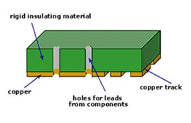
Single Side PCB
Single-Side PCB is the simplest and most common type of PCB. It was the first device used for the interconnection and assembly of electronic components forming a cohesive and functional operating system. The primary industry that uses these boards is the consumer electronics industry.
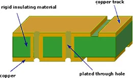
Double Side PCB
Double Side PCB have made circuit in 2 layer of different PCB side that both layer has connect by via PTH (Plated Through Hole) which depend on design this is more complex than Single Side PCB.
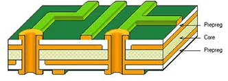
Multi Layer PCB
Multi Layer PCB have more layer than double side PCB, it has many circuit layer between Top side and Bottom side of PCB and also each layer can connect with via PTH (Plated Through Hole), this type is more complex than double side PCB.
Gerber file (RS-274-X)
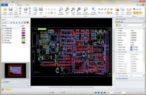
We offer a full range of printed circuit board capabilities to fit all of your PCB needs.Currently we accept 5 PCB file formats ( gerber file, .pcb, .pcbdoc .cam or .brd file format) for PCB fabrication. But if you design your boards with Sprint-Layout software, you can send the .lay6 file to service@pcbway.com for manually generating Gerber files.
- Gerber file format: RS-274-X
- Gerber file naming:
- GTL Gerber top layer
- GTO Gerber top overlay
- GTS Gerber top solder
- GBL Gerber bottom layer
- GBO Gerber bottom overlay
- GBS Gerber bottom solder
- GKO Gerber keepout layer
- DRD Excellon drill file
 1.6mm (Default)
PCB Board Thickness
0.4mm, 0.6mm, 0.8mm, 1.0mm, 1.2mm, 1.6mm, 2.0mm, 2.4mm
Please contact us if your board exceeds these.
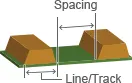
Min Track/Spacing
Min. Line Spacing & Min. Line Width: 4/4mil 5/5mil 6/6mil ↑

Min Hole Size
0.2mm 0.25mm 0.3mm ↑

Silkscreen
White, Black, None
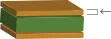
Finished Copper
1oz/2oz/3oz(35μm/70μm/105μm)
Inner Layer Copper Thickness:1oz/1.5oz(35μm/50μm)
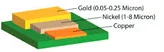
Surface Finishing
HASL with lead,HASL lead free,Immersion gold,Hard Gold ,OSP...
PCBWay Quality control
As the circuit boards are manufactured, and also after they are complete, we subject them to strict tests and checks:
- E-Test
- A.O.I. – Test (Automated Optical Inspection)
- X-ray (check registration accuracy for multilayers)
- CCD – Camera Controlled Drilling
- Impedance control
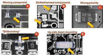
The testing of our SMD stencils includes:
Real-Time Process Control, monitors the cutting process for every aperture in real time
optical (sight) check
verification of manufacturing tolerances
 Angle position sensor carbon printing pcb carbon circuit board batch PCB printed circuit board
 Single-sided quartz glass substrate Alumina Ceramic PCBs Biomedical testing 3D printer insulation bed, ceramic substrate luminous keyboard motherboard, alumina pcb grating gear
 High frequency and high speed circuit substrate ceramic pcb Characteristic impedance 50Ω ceramic printed circuit board differential impedance 100Ω ceramic substrate pcb circuit board
 1.0mm Ceramic Circuit Board ENIG alumina circuit board High frequency and high speed printed circuit board ceramic pcb board